
TL;DR

Get the latest gadgets delivered free with Prime
- Fast, free delivery on millions of items
- Prime Video, Amazon Music and more included
- Member-only deals all year
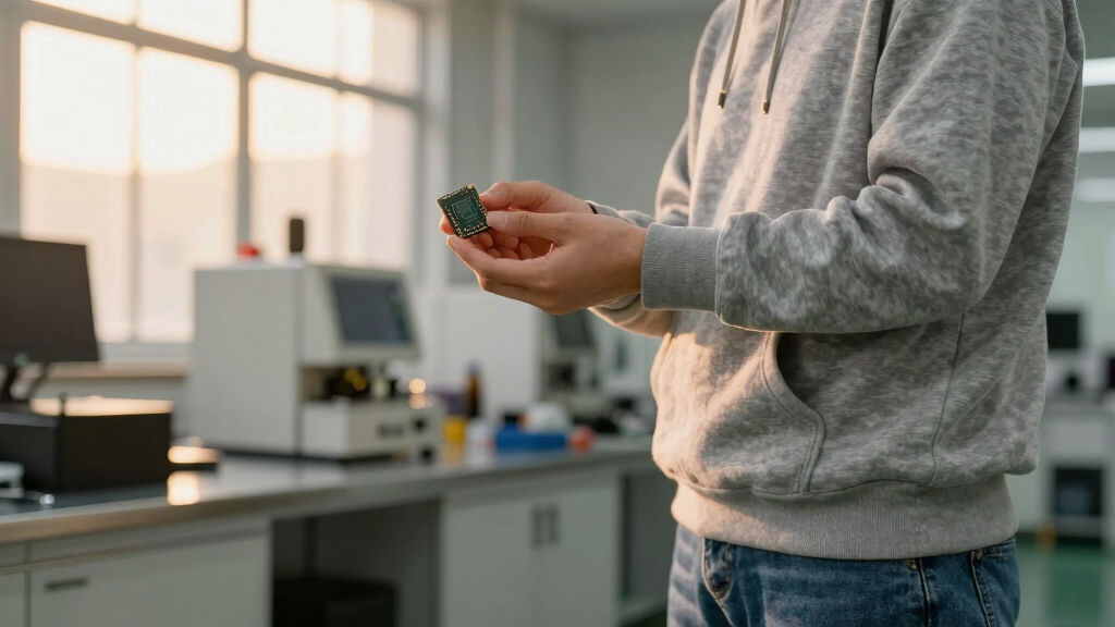
Jim Keller’s startup is building a factory to mass-produce small chip fabrication units. This development could significantly impact semiconductor manufacturing by enabling more scalable and accessible chip production.
Jim Keller’s startup has revealed plans to build a factory dedicated to mass-producing small-scale semiconductor fabrication units. This move aims to address manufacturing scalability challenges and reduce costs in chip production, marking a significant development in the semiconductor industry.
The company, whose name has not yet been disclosed, is developing a manufacturing facility designed to produce compact, modular chip fabs at high volume. According to sources familiar with the project, the factory’s goal is to enable faster deployment of fabrication plants, potentially transforming how chips are produced globally.
Jim Keller, a renowned chip designer and founder of the startup, confirmed that the project is in the early stages but intends to leverage innovative manufacturing techniques to make small fabs more accessible and scalable. The company aims to significantly reduce the capital expenditure associated with traditional large-scale fabs.
Potential Impact on Semiconductor Manufacturing Scalability
This development could democratize chip manufacturing by making fabrication plants smaller, more affordable, and quicker to deploy. If successful, it could lower barriers for new entrants, accelerate innovation, and help address global chip shortages. The move aligns with industry trends toward modular, flexible manufacturing solutions and could reshape supply chain dynamics.
semiconductor fabrication equipment
As an affiliate, we earn on qualifying purchases.
As an affiliate, we earn on qualifying purchases.
Industry Shift Toward Modular and Smaller Fabs
Over recent years, the semiconductor industry has faced increasing pressure to expand capacity amid rising demand and geopolitical tensions. Traditional fabs are extremely expensive and time-consuming to build, often costing billions of dollars and taking years to become operational. Recent efforts have focused on developing smaller, more flexible manufacturing units, but widespread adoption has yet to materialize.
Jim Keller’s background as a leading chip architect and his previous work at companies like Apple and AMD lend credibility to this initiative. His startup’s approach aims to leverage advances in manufacturing technology to create a new paradigm for chip production, potentially complementing existing large fabs or replacing some of their functions.
“Our goal is to make chip fabrication more accessible and scalable by producing small, modular fabs that can be deployed quickly and at lower cost.”
— Jim Keller
small chip fab manufacturing tools
As an affiliate, we earn on qualifying purchases.
As an affiliate, we earn on qualifying purchases.
Unconfirmed Details About Factory Capacity and Timeline
It is not yet clear what the exact production capacity of the factory will be or when the first small fabs will be operational. The company has not disclosed specific timelines or technical specifications, and the project remains in early development stages.
Further details about funding, partnerships, and technological innovations involved are still emerging, and industry experts are cautious about the timeline for commercial deployment.
modular semiconductor manufacturing units
As an affiliate, we earn on qualifying purchases.
As an affiliate, we earn on qualifying purchases.
Next Steps for the Startup and Industry Adoption
The startup is expected to provide more detailed plans and timelines in the coming months. Watch for announcements regarding pilot projects, funding rounds, and potential partnerships with manufacturing equipment providers or semiconductor firms.
If the project progresses as planned, the company could begin pilot manufacturing within 1-2 years, with broader deployment possibly following within 3-5 years. Industry adoption will depend on proving the technology’s scalability, cost-effectiveness, and reliability.
As an affiliate, we earn on qualifying purchases.
Key Questions
What exactly are small chip fabrication units?
Small chip fabrication units are modular, compact manufacturing plants designed to produce semiconductor chips on a smaller scale than traditional large fabs. They aim to be more flexible, cost-effective, and quicker to deploy.
Why is this development significant for the semiconductor industry?
If successful, it could lower barriers to entry, reduce manufacturing costs, and enable faster scaling of chip production, helping to address global shortages and foster innovation.
When might we see these small fabs become commercially available?
Details are still uncertain, but industry sources suggest pilot projects could start within 1-2 years, with wider deployment potentially within 3-5 years.
Who is Jim Keller, and why is his involvement important?
Jim Keller is a renowned chip architect with a history of designing influential processors at Apple, AMD, and other companies. His leadership lends credibility and technical expertise to the startup’s ambitious plans.
What challenges does this project face?
Key challenges include developing reliable manufacturing technology at small scales, securing funding, and convincing industry stakeholders of the viability and advantages of small modular fabs.
Source: hn
Halloween Picks
halloween
As an affiliate, we earn on qualifying purchases.